My implementation of the Jaguar on FPGA written from zero.
The goal was to made a more powerful Jaguar with the most possible compatibility, and without bugs. As different enhancement are made, some original program will need patches to run properly.
For a FPGA Jaguar fully compatible with the original, there is the Torlus one. You can find it here
The first version (v1.0) was made on an Altium NB3000 development board which has an EP3C40 CycloneIII FPGA. The Jaguar Core uses 99.99% of the available space of the FPGA.
I hadn't enough space into this FPGA to complete the implementation and to do all enhancement that I would like to do, so I bought a board with an ArriaV and made the v2.0 that give me enough space to finish the implementation.
The target FPGA for the final version will be a CycloneV.
The 68000 core is home made and have a pipelined instruction structure.
Each instruction is decomposed into :
| Step 1 | Step 2 | Step 3 | Step 4 | Step 5 | Step 6 |
|---|---|---|---|---|---|
| Read Instruction | Decode Instruction | Read Registers | Read Memory | Compute | Write Back |
Adding to that, almost all instruction execute each steps in 1 cycle.
This architecture gives the ability to execute up to one instruction by cycle.
The Cycle Table is here
You can find the Compatibility list here
| 68000 | Original | CycloneIII (v1.0) | ArriaV (v2.0) |
|---|---|---|---|
| Frequency | 13.295 MHz | 30 MHz | 50 MHz |
| Instruction Cache | none | 1 kBytes | 2 kBytes |
| Data Cache | none | none | planned for the v2.1 |
| Instruction Pipeline | none | yes | yes |
| Addr Bus Width | 24 bits | 26 bits | 32 bits |
| Data Bus Width | 16 bits | 32 bits | 64 bits |
| GPU | Original | CycloneIII (v1.0) | ArriaV (v2.0) |
| Frequency | 26.59 MHz | 60 MHz | 100 MHz |
| Internal Ram | 4 kBytes | 8 kBytes | 32 kBytes |
| Read/write Burst length | 2 | 256 | 256 |
| Register File structure | dual port ram | 1 write and 3 read ports ram | 1 write and 3 read ports ram |
| Internal Ram structure | one port ram | dual port ram | dual port ram |
| Addr Bus Width | 24 bits | 26 bits | 32 bits |
| Data bus Width | 64 bits | 32 bits | 64 bit |
| DSP | Original | CycloneIII (v1.0) | ArriaV (v2.0) |
| Frequency | 26.59 MHz | 60 MHz | 100 MHz |
| Internal Ram | 8 kBytes | 8 kBytes | 32 kBytes |
| Read/write Burst length | 2 | 256 | 256 |
| Register File structure | dual port ram | 1 write and 3 read ports ram | 1 write and 3 read ports ram |
| Internal Ram structure | one port ram | dual port ram | dual port ram |
| Addr Bus Width | 24 bits | 26 bits | 32 bits |
| Data bus Width | 16 bits | 32 bits | 64 bit |
| Blitter | Original | CycloneIII (v1.0) | ArriaV (v2.1) |
| Frequency | 26.59 MHz | 100 MHz | 120 MHz |
| Command list | 1 | 2 | up to 256 |
| Pipeline | none | yes | yes |
| Addr Bus Width | 24 bits | 26 bits | 32 bits |
| Data Bus Width | 64 bits | 32 bits | 64 bits |
| Object Processor | Original | CycloneIII (v1.0) | ArriaV (v2.1) |
| Frequency | 26.59 MHz | 100 MHz | 148.52 MHz |
| Instruction Cache | none | 2 kBytes | 2 kBytes |
| Pipeline | none | yes | yes |
| Addr Bus Width | 24 bits | 26 bits | 32 bits |
| Data Bus Width | 64 bits | 32 bits | 64 bits |
| Line Buffer structure | dual 360 x 32 bit ram | dual 512 x 32 bit ram | dual 1024 x 64 bit ram |
| Max Unscaled Pixel by cycle | 2 for 1 to 16 bpp 1 for 24 bpp | 2 for 1 to 16 bpp 1 for 24 bpp | 4 for 1 to 16 bpp 2 for 24 bpp |
| Max Scaled Pixel by cycle | 1 | 1 | 1 |
| Max Screen Resolution | 1382 x 625i @ 50 Hz 1400 x 525i @ 60 Hz | 800 x 600p @ 60 Hz | 1280 x 720p @ 60 Hz |
| Memory | Original | CycloneIII (v1.0) | ArriaV (v2.0) |
| Frequency | 26.59 MHz | 100 MHz | 133.33 MHz |
| Technology | DRAM | SDR SDRAM | DDR3 SDRAM |
| Available Memory | 2 MBytes | 64 MBytes | 256 MBytes |
| Interface Width | 64 bits | 32 bits | 64 bits |
| Max Bandwidth | 106 MBytes/s | 400 MBytes/s | 1 GBytes/s |
This board was made to fast program Jagtopus board.
It's composed of a FPGA, a SDCard, 2 buttons (reset and start prog) and 4 Jaguar slot.
There is 149 components on the board.
Three board exist.


The JagCFv3 is more powerful than the JagCFv2.
The JagCFv3 is composed of :
- Cyclone III FPGA
- 4Mbytes of Flash memory (to boot the jaguar and for libraries)
- 32Mbytes of SDRAM
- Compact Flash connector
- I2S output for audio streaming connected to Jaguar DSP
- UART input/output up to 3Mbps for remote debugging
- Two PS/2 connector for PC mouse and keyboard
- CAN bus connector for JagCF network
There is 204 components on the board.
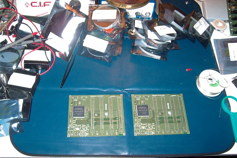
Four PCB exist but only two are yet soldered.


The JagCFv1 was too slow to do some interesting stuff.
Some developer (me too :p) wanted more POWA, so I started working on the JagCFv2.
It's the first version shown in public at the Atari Connexion 2006.
The JagCFv2 was composed of :
- Cyclone I FPGA
- Flash memory (to boot the jaguar)
- 8Mbytes of SDRAM
- External connector for future features like PS/2
One prototype was made.


RGC2006 demo : streaming of audio from CF with Real-Time Fluid Dynamics depending of the FFT computation.
AC2007 demo : 640x480 selection screen with various example (video, games...)
The JagCFv1 was the first try to do a CF interface on the Jaguar cartridge slot.
It was composed of a CPLD, FLASH memory (to boot the Jaguar) and the CF connector.
One prototype was made.

